How to use the circuit board. How to use a breadboard for solderless mounting. Main types of breadboards
Hi all. Today we will talk about solderless breadboard or about breadboard as the bourgeois call it. This board, so to speak, is included in the list of mandatory tools that an electronics engineer should have (whether it be a young brainmaker who is just taking his first hesitant steps or a hardened and experienced brainchild).
Knowing what prototyping boards are, how and where such tools are used, will help you in developing and setting up your own projects of various electronic homemade.
The first boards looked like this:

Metal racks were attached to the base, on which wires and contact leads of the elements were subsequently fixed (simply wound).
It is good that technological progress does not stand still - because thanks to its influence, we can use such wonderful tools.

As opposed to a solderless breadboard, you can set these up (they are much cheaper and are made based on the required parameters).


However, when mounting on a solderless board, you do not need a soldering iron / solder. In addition, you will avoid the difficulties associated with desoldering parts on the surface of the board.
rule good manners, and common sense, there has always been and remains prototyping electronic circuits. It is important to know how the device will behave with certain specific parameters before assembling the finished device.

In addition, using a solderless board, you can check the performance of new components and radio components.
Consider the structure of a solderless board

Let's look at the drawing of the board. It consists of rows of metal plates (rails).
The rails, in turn, consist of clamps into which the “legs” of the radio components are installed. All 5 holes in a row are connected together.


Now let's turn our attention to two vertical / horizontal stripes (it depends in which position to look), which are located separately (along the edges) - these are the power plates. All nests of one long plate are connected to each other.
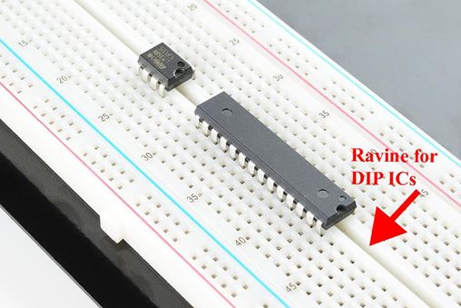
The central groove isolates the sides of the board. The width of this band is fixed by the standard. It allows you to install DIP-circuits in such a way that each pin is installed in a separate rail and allows you to connect up to 4 external pins.

The boards are marked with alphabetic and numeric sequences. These designations help you navigate when installing components in order to exclude erroneous connections (which may result in the circuit not working or failure of individual parts).
They also produce boards that are made on separate stands with special clamping terminals. They are used to connect the power supply to the board.

If you pay attention, some boards have special grooves and protrusions (they are located on the sides). With their help, you can combine boards and create a work surface of any size.

Also, on some boards, a self-adhesive base is applied on the back.
The figure shows a way to "power" the board from the Arduino.

If you come across a board with power supply terminals, you need to connect them to the lines on the breadboard using conductors (jumpers). The terminals are not connected to any line. To connect a wire to a terminal, remove (unscrew) the plastic cap and place the end of the wire into the hole. Reinstall the cap. Usually two terminals are used: for power and for ground.
Now the matter remains small, we connect an external power source. This can be done with:
- jumpers;
- "crocodiles" or ordinary wires;

- power stabilizer modules that are produced for solderless boards.

Thank you for your attention. To be continued 🙂
LiveJournal did not swallow the second part of the post as a whole, either, so I'm breaking it into two more parts. Here Part 3 - The very first laboratory work , .So, the first laboratory lesson - "Assembling simple electronic circuits based on microcircuits of a low degree of integration" - a few practical exercises to get acquainted with the basics of digital logic:
- familiarity with breadboards and basic circuitry elements (LEDs, diodes, capacitors, etc.),
- basic operations of Boolean algebra in physical execution,
- logical elements (gates),
- dynamics in the form of a simple timer,
- elementary output devices (diode display)
triggers (flip flops) from the first acquaintance fell out and were left for better times.
Input assumptions about learning objects:
- have vague memories of the basics of electrodynamics from the course of the school curriculum (voltage plus or minus, current flows, you can add resistance)
- have a good understanding of at least the basics of discrete mathematics (Boolean algebra) and programming (procedural thinking), so that after passing the introductory exercises, they can intuitively feel that large discrete systems of any complexity can be built from the presented simple physical elements of logic, in which complex abstract ideas that can be formulated in the language of logic have already been implemented.
Actually laboratory work
1. Main details—
breadboard, diodes and LEDs
The breadboard allows you to create electronic circuits of any configuration without the use of a soldering iron - simply by sticking the legs of the circuit elements into the holes of the board. This is possible due to the way these holes are connected inside under the plastic by conductors. Along the edges there are horizontal stripes with plus and minus along the entire length of the board - if you plug the wire from the battery (for example, plus) into one of the holes anywhere, plus will be fed along the entire length of this strip and you can "feed" from it by plugging the wire into any other hole of the same horizontal strip.
The basis of the board is a sequence of vertical (if you look at the photo below) conductor strips with five holes above each. If you stick two wires into two holes above the same vertical strip, they will be connected in a chain (the same as twisting their legs directly). Two adjacent strips are not connected in any way, so by sticking one ends of the elements into one vertical strip, and sticking the other ends of the same elements into others, you can build serial circuits of any configuration. After that, a plus is supplied from the horizontal strip with a plus to one of the vertical strips through the wiring, and with horizontal stripes with a minus, a minus is supplied to another part of the circuit through another wiring, and the whole circuit starts to work.
If it is not very clear now, everything will become clear after the first experiment with the LED.
For the direction of the current in the diagrams, it is customary to take the direction from plus (+) to minus (-).
Note: do not confuse the "conventional" current direction (from plus to minus) with the direction of the physical flow of electrons that run from minus to plus - i.e. in the opposite direction - in some literature (including in the book tron.ix in one of the first pictures - hence the remark) - the direction of the electron flow is used, in the other - the "conventional" direction of the current - this is due to traditions and some other nuances - electrical circuits it is more convenient to read using the "conventional" plus->minus direction, so we will use it everywhere.
A diode is a conductor that passes current in only one direction - from plus (+) to minus (-), and does not pass from minus (-) to plus (+). In the diagrams, the diode is indicated by an arrow resting on a vertical line, the arrow indicates the direction of current allowed by the diode. The leg of the diode, which in the current passing mode must be connected to the plus is called anode, which to the minus - cathode.
An LED is the same diode, only in the current transmission mode (when a plus is applied to the anode and a minus to the cathode), it shines with a light bulb, and in the non-transmission mode it does not shine. In the diagram, the LED is also indicated as a conventional diode, only the arrow is circled. The anode of the LED is a long leg (we apply a plus to it), the cathode is short (we usually connect it to a minus). On all the diagrams in the lab - in the photo and video - the long leg is on the left, and the short one is on the right.
2. Determination of boolean values TRUE / FALSE on the selected section of the circuit — LED as current value indicator
Boolean variables are determined by the voltage level in the section of the circuit from which we take the value. For TRUE=1=HIGH we accept the value plus (+) ("voltage HIGH"), for FALSE=0=LOW we accept minus (-) or ground ("voltage LOW").
In order to personally check the current boolean value in the selected area, you can use the LED - connect the anode (long leg) to the point of reading the value, and connect the cathode (short leg) to the minus. If a plus (+) is applied to the anode connection point, i.e. the read value must be TRUE, the current will flow from the anode to the cathode through the LED and its light will light up. If there is a minus or ground at the anode connection point, the current will not flow, the light will not light up - the value taken is FALSE.
Note: It is not recommended to connect the LED directly to the battery without an intermediate resistance or if the connected resistance is too low, because otherwise, it may burn out due to too much current for which it was not designed (for a while it will glow, but it will get very hot and eventually burn out). With a resistance of 500 ohms (which was previously chosen as "weaker"), nothing threatens the LED.
Task in the audience: draw an LED wiring diagram on the board and ask the group to implement it on breadboards. At this moment, a nuance specific to work in the audience is immediately revealed. There are two pictures in the tron.ix book for each exercise - one shows the logical connection diagram, the second shows a breadboard with holes and all the necessary elements so that you can see which legs are stuck where, etc. Sitting at home with a book, it's easier to look at the second picture and just repeat the drawing from the book on a live breadboard. In the audience with big amount a person does not roll this trick in any way - a distinct photorealistic image of a breadboard with all the holes and with all the elements stuck in a pile is quite difficult to draw on the board with a marker, so it’s easier to draw circuit diagram, and students themselves are already delving into how to make its physical embodiment on a breadboard. The first task with a simple LED and resistance took about 10 minutes. this was the first acquaintance with the device of the breadboard (the connection diagram of the holes inside the board during the first task, by the way, can not be erased from the board) and a second meeting with the basics of electrodynamics after a long separation - for example, some people first decided to put the legs of the LED directly into the holes of the strips for power supply (both in plus), but after some clarifications and clarifications, everyone delved into the topic, and on the following tasks, the process of converting a logical circuit into a physical circuit was already much more fun.
3. Truth table and OR operator
As shown in the previous exercise, as variables
, which can take boolean TRUE/FALSE values, we can take certain areas chains - because V different conditions the voltage on the same section can be both HIGH (+) and LOW (-) - hence the term " variable" - the possibility of assigning a value.
Moreover, if we build some combination of electrical elements (such as diodes, resistances, etc.) between two sections of the circuit, this intermediate combination (or circuit) can affect what value will be taken in the second (output section) of the circuit, depending from the current value on the 1m (input) section of the circuit. Those. this intermediate circuit essentially converts one or more values on the incoming chain legs to a new value on the outgoing chain leg according to a certain rule. Because values on all sections (incoming and outgoing) can take the value TRUE / FALSE, i.e. they are boolean variables , we can take the intermediate converter circuit as a normal boolean operator (namely, for its physical implementation).
In discrete mathematics, any operator is given by its truth table, which lists all possible combinations of values of variable parameters (for two input variables: 11, 10, 01, 00) and indicates the value of the result of the operator's action for each of the combinations (for two input variables, this is there will be 4 values of ones and zeros).
As indicated at the beginning - it is assumed that the audience should be familiar with at least the basic concepts of discrete mathematics, which include truth tables - this assumption was confirmed in the audience - it was not necessary to explain for a long time what a truth table is - everything and they were already aware of it.
As a first example, consider the physical implementation of the elementary Boolean operator OR. Its schematic diagram looks like this:
You can find out how its truth table looks like by finding the definition of this operator in a textbook on discrete mathematics or by assembling the above circuit on a breadboard - to set values for the input variables-parameters A and B, you can stick the corresponding wires A and B into compartments (+) (TRUE= 1) or (-) (FALSE=0), while the result of the operator's action on the section of the chain Q will be seen from current state red LED (on - the operator returned Q=TRUE=1, off - Q=FALSE=0). We will of course use the second option.
Comment: Why is this physically happening? this case it is quite simple to understand - when the anode of any of the input diodes is connected to the positive (A=1 or B=1), the circuit closes and a non-zero voltage is applied to point Q (to which the LED anode is also connected) - the light is on - Q=HIGH=TRUE . If none of the anodes A and B is connected to the positive (+) (i.e. A=0=FALSE and B=0=FALSE), there is nowhere to take the voltage in the circuit from. the area with the plus is completely isolated - that's why the light bulb cannot burn and Q=LOW=FALSE. But I don’t think it’s necessary to focus on this mechanism here and on the following diagrams during classes in the classroom, because. the brain of students at this moment is busy absorbing and assimilating information that the Boolean operators familiar to them from discrete mathematics and programming can behave in the same way as living light bulbs in the circuit that they have just assembled from several wires, i.e. give the same truth tables. Therefore, it is more important to focus attention precisely on the observation of the fundamental possibility of the existence of the transition point "physics in the face of electrodynamics" -> "abstraction of discrete mathematics". An additional immersion in electrodynamics can damage this process or, in the end, simply will not be perceived as it should be - an explanation of the details of the mechanism of this process can be left on independent work, for a separate lesson later or keep in mind in case of additional questions from the audience (if suddenly someone still learns new information quickly enough and wants additional explanations).
4. AND operator
Almost nothing new compared to the previous exercise - just build an operator AND according to the scheme.
Comment: Pabout the physics of the process - if we close one of the cathodes (A or B) to minus (-), the current will flow directly from plus to minus through the network section through the corresponding diode, and to the network section Q (with this configuration it turns out to be connected in parallel to the diode) forces the current is simply "not enough" to light the bulb (i.e., set Q=TRUE). when circuit sections are connected in parallel, the current is distributed inversely to the value of the internal resistances of these sections (for example, if one of the diodes is connected through an individual resistance, then the focus will not work - the current will flow through both channels).
Comment: in the classroom - when building a circuit, it is desirable to fit it in the left half of the breadboard, because further we will use it for the composite NAND operator.
Returning to the analogies of input-output interfaces and black boxes - the transistor is just an example of such a box, the device of which is basically unknown to us. If everything is more or less intuitive with resistances or diodes - their work can be based, for example, on the physical and chemical properties of the conductivity of the materials from which they are made, then the logic of the transistor's behavior should obviously be implemented through some more tricky mechanisms and combinations of materials. But in order to use it within the framework of the course, it is not necessary for us to delve into this device in general (and we will not do this) - it is enough to know that a plus must be applied to the collector, a minus to the emitter, and conductivity can be turned on / off plus or minus on the base.
Comment: Pabout the physics of the process - almost similar to an AND circuit - if the base is on the minus (A=FALSE), the transistor is closed, the current can only flow through the Q section with the diode - Q=TRUE. If the base is connected to the positive (A=TRUE), the current starts to flow through the transistor, its power is no longer enough for the Q section connected in parallel - we get Q=FALSE.
Comment: in the audience - pWhen building a NOT circuit, we do not disassemble the AND circuit from the previous exercise - we build NOT on the right side of the breadboard, because in the next exercise, we will make a compound NAND operator out of them.
6. Combining logical elements into a logical circuit
—
NAND operator as AND+NOT
A very simple technically and conceptually important exercise is to combine two statements into one compound statement by feeding the output of one statement to the input of another. We insert the "A" wire from the NOT operator into the hole on the output subnet "Q" of the AND operator (red LED cathode AND) - received the NAND operator - input parameters - wires "A" and "B" from the AND operator, the output result is a green LED " Q" of the NOT operator. We leave the intermediate red LED-indicator from the AND operator for clarity - when changing the values of the input parameters A and B, the red and green LEDs must always be in anti-phase (only one of them is lit).
(The audience combined OR and NOT in NOR, but for a smooth transition to the next exercise with the 4011 module, it is better to do NAND)
You can take a break here.
7. Introduction to Digital Logic Modules
—
4 NAND operators inside
module 4011
A new important conceptual element is the digital logic module (logic gate) using the 4011 gate as an example, which contains 4 NAND digital logical operators inside - this time it is a black box in the literal sense - a black rectangular parallelepiped on all sides (except for the silver inscription ) with protruding legs that fit perfectly into the breadboard (if you don’t forget about the nuance with the DIP package) - some of them are an input interface, some are an output interface.
Obviously, such logical modules should greatly facilitate the life of circuitry, because. raise it one level higher in the hierarchy of simplifying abstractions - to see this, it is enough to compare the size of element 4011 (which contains 4 NAND operators) and the scheme of one NAND operator, which we assembled by hand above. In order to use a ready-made logic module, it is enough to look at its schematic diagram and find out which legs are responsible for what.
In the case of 4011, in order to use, for example, the first NAND operator out of 4 available, you can connect the input wires A and B to pins 1 and 2, respectively, and the output wire Q to pin 3 (well, supply power - minus (-) to pin 7, plus (+) on leg 14) - the truth table for Q will show the effect of the NAND operator exactly as in the previous example.
(at the end of the video, a small blot - the last line should be written "0, 0, 1" instead of "1, 1, 1")
It is clear that a large number of such logical elements have been created for all occasions (from basic logical operators to pulse generators like 555 or a 7-segment display driver 4511) - as in the case of 4011, in order to use them, it is not particularly important to know how they are arranged inside - just look at the documentation about what and under what circumstances can be served and what can be removed from its paws. In general, almost complete analogy with libraries of ready-made functions or objects in the programming world.
(If you do not disassemble the NAND from the AND + NOT exercise and fit the NAND from 4011 next to it, then you can make sure that the bulbs of both NAND "in with the same input values \u200b\u200bshould give the sameweekendvalues, i.e. scheme assembled by hand of resistors, diodes and transistors, gives the same result as the circuit stitched inside the black module 4011).
8. Timer with two NAND elements and a capacitor
And again important new element- periodic signal generator - timer (Clock). Up to this point, all the assembled logical circuits were static - when the necessary signals were applied to the input subnets (A and B), their value was uniquely converted through a sequential chain of logical operators into the value of the output signal Q, which, without manually changing the values of the input signals (A and B) ( for example, manually poking the wire from plus to minus) will not change in any way. The element "timer" (or "clock" - in tron.ix it is called Clock, while there was also an additional special element Timer) adds dynamics to this process - the value of the output signal of the timer independently changes from HIGH (TRUE) to LOW (FALSE) and back with a certain frequency, and at the same time, a person does not participate in this process in any way (there is no need to poke the wire from plus to minus with your hands).
In conjunction with triggers (flip-flops - elements that can "remember" their value), in the future this will allow building finite automata that will sequentially transition from one state to another for each "cycle" of the timer.
The sequence of output values HIGH / LOW at each moment of time is shown as a broken line on a special graph - in the future, such graphs will be more familiar in the following labs when simulating the behavior of finite automata.
The timer can be assembled from 2 NAND elements (taken from logic element 4011) and capacitor C1 (new element in the diagram - see note below). The capacitor has two legs - one is longer (conditional plus), the second is shorter (conditional minus), but apparently which side to stick the capacitor in at least this circuit does not play a special role, because. their polarity still changes in the process of oscillation (that's the whole point).
Comment: according to the physics of the process - a new electrical element of the circuit, without which the timer could not work - a capacitor - it is arranged quite simply inside - two plates isolated from each other - if a charge (+) is accumulated on one of them, and a minus (-) is left on the second (i.e. the capacitor will charged) and then connect the legs to different parts of the circuit, current will flow through the circuit from plus to minus until the charges are equal (capacitor discharged). After discharging, the capacitor can be charged again by applying a plus to one plate and a minus to the other. In this scheme, with the help of two NAND elements, a process is organized in which the capacitor will constantly be charged, then discharged at a certain frequency and thus generate a periodic pulse. When half of the capacitor C1, connected in the circuit to output 3 of the 1st NAND element through the resistance R1, is charged with positive (+), inputs 1 and 2 of the 1st NAND element are TRUE (+) and TRUE (+), which at output 3 gives the value FALSE (-) (see NAND truth table) and thus the capacitor has the ability to discharge its plus (+) into this negative section of the circuit through the resistance R1. After the positive (+) charge of the capacitor is completely lowered, those. turns into minus (-), inputs 1 and 2 of the 1st NAND element logically receive the values FALSE (-) and FALSE (-), which accordingly changes the value of output 3 to TRUE (+) - as a result, we get that the current is already flowing in opposite direction back into the capacitor until it recharge back to plus (+) - i.e. we get to the original state. And so in a circle - the frequency of the process will depend on the capacitance of the capacitor (this is his physical characteristic) and resistance force R1 (F=1/R1*C1). You can, as an additional experiment, replace R1 with a resistance with a different value and make sure that the blinking frequency of the light bulb changes.
Comment: to generate a periodic signal on the circuits, you can use a special logic module 555, but experiments with it were not included in the lab.
9. Output device
—
seven-segment LED display
As a relaxing exercise in the end - acquaintance with the first "human" output device - a seven-segment diode display. In fact, the same LED bulbs, but by supplying current to the desired segments of the screen, you can "draw" on it all the numbers from 0 to 9 and some letters.
There is nothing special to tell about the device - for a general-anode display, you need to apply a plus to the leg (anode) common to all segments, and minus to the legs of the desired segments; for a general cathode display - on the contrary, on the leg (cathode) common for all segments, minus, and on the legs of the desired segments - plus.
But I think the main effect is produced by the very fact that the display for the first time shows a way to convey internal state of the assembled scheme to a person in the form familiar to him (in readable numbers and letters), i.e. ultimately sets the goal to which any assembled circuit- do something with the output device (a black box without an output device is a "thing in itself", from which it is not clear what is the use and why it is needed).
Everyone really liked the seven-segment diode displays with a common anode. Even instead of dispersing after a long lesson, a spontaneous decision was made to make the name of the group "10-PM" out of them (Applied Mathematics 2010 year of admission - the letter "M" was made in the form of the number "3" turned on its side) and shoot it on photo.
10. Note- dropped trigger
The list of exercises did not include the last important conceptual element - this is a trigger (flip-flop) - a circuit element that can remember the last value set to it. Without this element, it would be impossible to build finite automata (in particular, processors). Initially, it was planned to include an introduction to the understanding of a trigger using the RS trigger as an example (because it has a rather simple scheme), but in the course of the lesson it became clear that the amount of new information perceived at a time had already reached the digestibility limit. Therefore, acquaintance with flip-flops (a simple RS-trigger and a more important D-trigger) has been transferred to the following laboratory work immediately before using them, when we will consider finite automata specifically.
Conclusion
My impressions of the laboratory work as an Applied Mathematics graduate and Java programmer. The most important result is that this laboratory work showed the existence of a superstructure of the foundations of discrete mathematics (Boolean algebra) over school electrodynamics (of which I personally had little left except vague memories of Ohm's law) - the realization of this fact opens the way to understanding the principles of construction more complex electronic systems, which are based on the same discret.
From a practical point of view, playing with light bulbs on breadboards turned out to be quite important for the visual accelerated assimilation of new information, but I personally wouldn’t undertake the implementation of some relatively complex projects, having only breadboards and a scattering of different logic gates - after all increasing the complexity of the circuit, the process of connecting wiring on the circuit becomes quite tedious and time-consuming, while the complexity (and hence the value of the project) of the assembled system will be quite physically limited - the breadboard area can be increased, but how to do "code refactoring" or look for errors, when a thousand wires stick out from one heap, I can hardly imagine (although judging by the information on the Internet, someone manages to put entire processors on them, so I won’t say so categorically) - while the question of creating project documentation and converting a prototype thus assembled into a document format that could be used for mass production is not considered at all. A completely different matter is FPGA chips (FPGA) with programmable digital logic (they are based on all the same basic elements that were considered in the current lab, but the process of manipulating them is organized in a qualitatively more high level) - acquaintance with them immediately expands the boundaries for fantasy in choosing the goals of possible projects by orders of magnitude - the first acquaintance with them is planned for the next laboratory work.
All people in the world, young and old, know that before you create something, you must first create a model of this “something”, be it a model of a building, a stadium, or even a small rural toilet. In electrical engineering, this is called a prototype. A prototype is a working model of a device. Therefore, experienced electronics engineers, before assembling a device according to a scheme on the Internet, laid out by someone and do not understand why, must make sure that this scheme really works. Therefore, the circuit must be quickly assembled and made sure that it works, that is, to assemble layout. Well, in order to assemble it, we just need bread board.
Types of breadboards
Thick cardboard
A long time ago, when you were not even in the plans, our grandfathers, and maybe grandmothers, you never know :-), used thick cardboard. This is the fastest and cheap way schema checks. Holes were cut in the cardboard for the conclusions of the radioelements and, on the other hand, they were connected with the help of wires and other elements, if they did not fit on the front side. It looked something like this:
A is the front side, B is the reverse side.
Everything would be fine, but you had to solder the conclusions, make sure that nothing closes anywhere, and while you are “sculpting” this circuit, you can even inadvertently get confused :-). Yeah, it's not pretty either.
Homemade breadboards
I still found these times on the radio club. Back then we made breadboards ourselves. They took a sharp cutter and cut squares on a foil textolite. Then they were covered with solder.

If it was necessary to connect the tracks somewhere, we simply made jumpers between the squares with a drop of solder. It turned out good quality and beautiful. If it was too lazy to solder the radio elements to a normally wired board with tracks, they simply left it as is and used the device.
Disposable breadboards
Manufacturers still “sniffed” this business, or, as they say in economics, demand creates supply. Ready-made mock-up scarves began to appear one-sided and even double-sided for any size and taste.


By the way, they can be found on Ali immediately whole set .
The holes are very conveniently matched to the size of the pins of the microcircuits, as well as other radio elements. Therefore, it is very convenient to assemble and test an electronic device on such breadboards. And yes, they are inexpensive.

back side such breadboards already with ready devices will look something like this:

What are the disadvantages of these breadboards? Still, it is better to use them once, because with repeated use, patches can fly off from them, which will lead to its unsuitability.
Solderless Breadboards
Progress walks with its confident step in our world, and now the market has appeared solderless breadboards.
They cost a little more than simple disposable breadboards, but to be honest, it's worth it.
They are very convenient in terms of installing parts, as well as their connection with each other. Wires no larger than 0.7 mm and no less than 0.4 mm in diameter can be inserted into such breadboards. To find out which holes and tracks are ringing among themselves, we check this whole thing. To design large circuits (suddenly you will be developing some kind of hadron collider control unit), you can add the same breadboards back to back. For this there are special ears. One move, and the breadboard will become a bit larger.


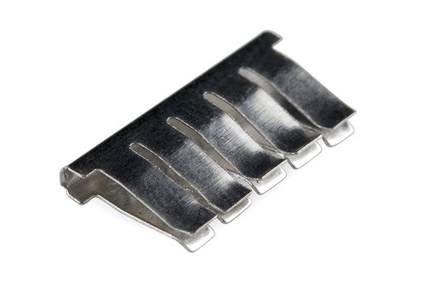
Well, what breadboard can be without connecting wires? Connecting wires, or jumpers ( from English- jump), are needed to connect the radio components on the breadboard itself.

A little later, I bought these jumpers from Aliexpress. They are much more convenient than wire:
.JPG)
Everything is simple here, we take the jumper and insert it with a slight movement of the hand


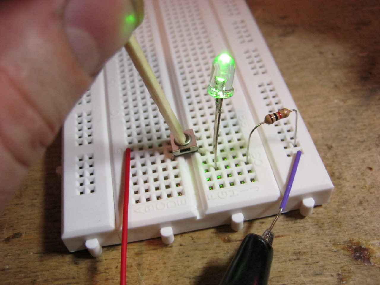
Let's assemble the simplest circuit for turning on an LED through a button on a breadboard

This is how she will look

Set the power supply to 5 volts and press the button. The LED lights up bright green. So the scheme is workable, and we can use it at our discretion.
Conclusion
Solderless breadboards are taking over the world. Any scheme on them can be assembled and disassembled in a matter of minutes. After assembling and testing the circuit on a breadboard, you can safely proceed to assemble it in its pure form. I think that every self-respecting electronics engineer should have such a breadboard. But keep in mind, it’s better not to check circuits with a large current in the circuit, since the contacts of breadboards can simply burn out - Joule-Lenz law. Good luck with your development and design radio electronic devices!
Where to buy a breadboard
A breadboard with flexible jumpers and even a ready-made 5 Volt power supply can be immediately bought as a kit on Aliexpress. choose to your taste and color!

If you don’t want to, then the easiest way would be to buy a one-time breadboard and assemble a finished device on it:
There is a factory breadboard of the following type:
I don't like her for two reasons:
1) When installing parts, you have to constantly turn back and forth in order to first put the radio component, and then solder the conductor. On the table behaves unstable.
2) After dismantling, the holes remain filled with solder, before next use boards need to be cleaned.
Searching the Internet different kinds breadboards that you can make with your own hands and from available materials, came across a few interesting options, one of which decided to repeat.
Option number 1
Quote from the forum: « For example, for many years I have been using these homemade breadboards. They are assembled from a piece of fiberglass, into which copper pins are riveted. Such pins can either be bought on the radio market, or you can make yourself from copper wire with a diameter of 1.2-1.3 mm. Thinner pins bend too much, and thicker pins take too much heat when soldering. This "dummy" allows you to reuse the most shabby radio elements. Connections are best made with a wire in fluoroplastic insulation MGTF. Then once made ends will last a lifetime.
I think this option suits me best. But fiberglass and ready-made copper pins are not available, so I'll do it a little differently.
Copper wire was extracted from the wire:

I cleaned the insulation and, using a simple limiter, made pins of the same length:

Pin diameter — 1 mm.

For the basis of the board took plywood thickness 4 mm (the thicker, the stronger the pins will hold):

In order not to suffer with the markup, I pasted lined paper on the plywood with adhesive tape:

And drilled holes with a pitch 10 mm drill diameter 0.9mm:

We get even rows holes:

Now you need to hammer the pins into the holes. Since the diameter of the hole is smaller than the diameter of the pin, the connection will be tight and the pin will be tightly fixed in the plywood.

When driving the pins under the bottom of the plywood, you need to put a metal sheet. The pins are clogged with light movements, and when the sound changes, it means that the pin has reached the sheet.
So that the board does not fidget, we make legs:

We glue:

The breadboard is ready!
Using the same method, you can make a board for surface mounting (photo from the Internet, radio):

Below, for completeness, I will give a few suitable designs found on the Internet.
Option number 2Pushpins with a metal head are hammered into a piece of the board:

It remains only to tin them. Copper-plated buttons are tinned without problems, but with steel ones. 
For the construction and debugging of prototypes of the most various devices arduino uses breadboards (another name is solderless circuit boards and breadboard). They come in several varieties and differ in size and some other design features. Breadboards can help both novice engineers to create simple circuits, and when prototyping complex devices. What is a breadboard and how to use this device will tell this article.
Rarely what real project Arduino contains less than 5-10 elements interconnected. Even in a simple well-known beacon circuit, 2 elements are used, an LED and a resistor, which must somehow be connected to each other. And this is where the question arises of how to do it.
To date, there are the following main mounting methods that are used in electronics and robotics at the prototyping stage:
- Soldering. For this, special boards with holes are used, into which parts are inserted and connected to each other by soldering (using a soldering iron) and jumpers.
- Cheat. According to this technology, the contact connections of devices are combined with a prototyping board by winding a clean wire to a pin contact.
by the most modern version for prototyping is a solderless breadboard, which has undeniable advantages:
- The ability to carry out debugging work a large number of times by changing the modification of circuits and methods of connecting devices;
- The ability to connect several boards into one large one, which allows you to work with more complex and large projects;
- Ease and speed of prototyping;
- Durability and reliability.
The English version of the solderless breadboard name is breadboard.
Breadboard Schematic
To know how to use a breadboard, you need to understand how it works.
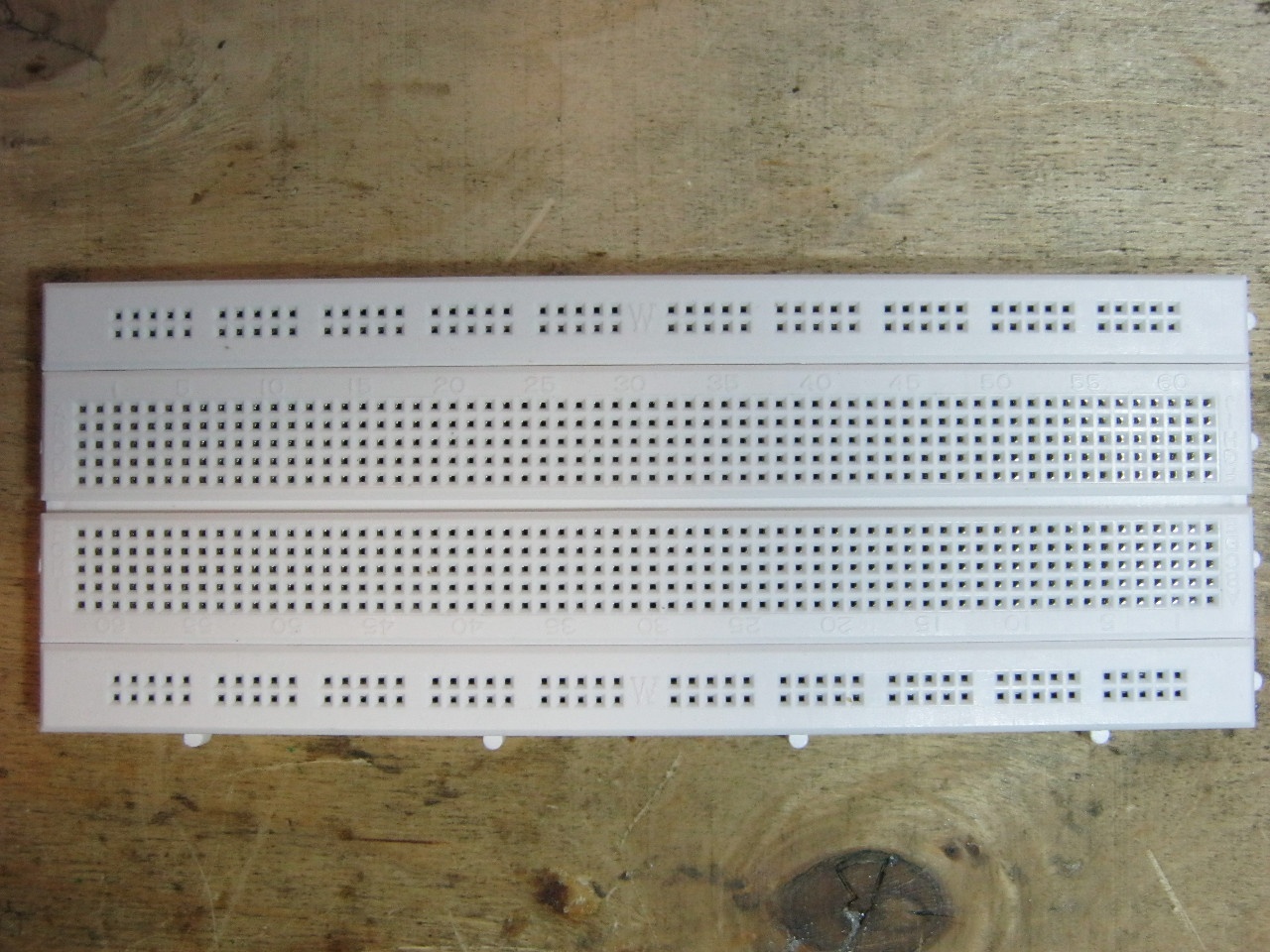
The solderless mount breadboard has a plastic base with multiple holes (standard spacing is 2.54mm). Inside the structure are rows of metal plates. Each plate has clips that are hidden in the plastic part of the unit.
The inclusion of wires is carried out precisely in these clips. When connecting a conductor to one of the individual holes, the contact is simultaneously connected to all other contacts of the individual row.
It is worth noting that one rail contains 5 clips. This is a common standard for all solderless boards. That is, up to five elements can be connected to each rail, and they will be interconnected.
It should be noted that although there are ten holes in each row, they are still divided into two isolated parts, five in each. Between them is a rail without pins. This design is necessary to isolate the plates from each other, and allows you to simply connect chips made in DIP packages.
Some breadboards also include two power lines on each side. Typically, the "red line" is used to supply "+" voltage, "blue" - for "-". Due to the presence of two power rails, two different voltage levels can be supplied to the board.
To simplify orientation, the breadboard is also marked with numbers and letters, which can be used as a guide, creating, for example, instructions for connecting.
Main types of breadboards
Prototyping boards differ in the number of pins located on the panel, the number of buses and the configuration. There are also prototyping boards in which the contact connections are made by soldering, but working with them is more difficult than with solderless devices.
Depending on the characteristics, the most common types are:
- For the assembly of large microcircuits, solderless boards with 830 or 400 holes are mainly used. For connecting several components and supplying wires to the necessary points - for 8, 10, 16 holes;
- With the presence of grooves for clutching boards, which allow the implementation of fairly large projects;
- With the presence of self-adhesive on the base for secure attachment to the device;
- With symbols printed on the board for connecting devices.
Depending on the cost and manufacturer, the package may also include additional accessories - jumper wires, various connectors. But the main quality criterion is always the number of contact connectors and their technical characteristics.
How to use the breadboard
The breadboard is pretty easy to use. When creating a pattern in holes on plastic case inserted necessary elements- capacitors, resistors, various indicators, LEDs, etc. The width of the connectors allows you to connect conductors with a cross section of 0.4 to 0.7 mm to the contacts.
The simplest example of creating a circuit prototype using a breadboard would be this implementation:

To assemble it, you need to take:
- Breadboard (breadboard);
- wires for connection;
- 1 LED;
- clock button;
- resistor with a nominal resistance of 330 ohms;
- battery type "Krona" 9V.
The plus of the battery is connected to the positive bus, and the minus to the negative. If the circuit is assembled correctly, then when you press the button, the LED will light up.
Attention! Solderless breadboards are absolutely unacceptable to use with a voltage of 220V!
Breadboards are optimal for creating almost any digital circuits and are not intended for assembling analog circuits with high resistance sensitivity. In their practice, they are often used by both beginners who learn the basics of circuitry, and experienced professionals due to ease of installation and High Quality connection of working contacts.